----------------------------------------------------------------------------------Welcome To this Blog--------------------------------------------------------------------------- I want to share my knowledge about Robotics Basics.Sensor Design.mechanical Design.*For any query,feel free to mail or add comment.
Tuesday, November 15, 2011
Sunday, November 13, 2011
IR REMOTE CONTROL
INFRA RED TRANSMITTER RECEIVER
Synopsis: The IR remote control circuit can be used for any switching function. This circuit is absolutely free from ambient light interference and provides control range of about 6 meters without the use of any focusing lens.
Transmitter:
In the transmitter section we have to generate a 38khz square waveform with the help of an astable multivibrator. So we use IC555 to implement an astable multivibrator and generate a 38 khz square waveform.
INTERNAL STRUCTURE OF IC 555
Description of the above circuit: The circuit consists of two comparators, an SR flip flop and a switch. One power supply (Vcc) is required for operation, with supply voltage typically 5 volt. A resistive voltage divider, consisting of three equal valued resistors labeled R1 is connected across Vcc and establishes reference voltage for the two comparators. These are Vth=(2/3)*Vcc for comparator1 and Vtl=(1/3)*Vcc for comparator2.
SR flip flop also called latch is a bistable circuit having complementary outputs. In the set state,the output Q is high and in the reset state the output Q is low. The flip flop is set to 1 by applying a high level to its set input terminal and reset by applying a low level to reset input terminal.
Astable Multivibrator Operation:
For explaining the operation of the timer 555 when Q is low or output VOUT is high, the discharging transistor is cut-off and the capacitor C begins charging toward VCC through resistances RA and RB. Because of this, the charging time constant is (RA + RB) C. Eventually, the threshold voltage exceeds +2/3 VCC, the comparator 1 has a high output and triggers the flip-flop so that its Q is high and the timer output is low. With Q high, the discharge transistor saturates and pin 7 grounds so that the capacitor C discharges through resistance RB with a discharging time constant RB C. With the discharging of capacitor, trigger voltage at inverting input of comparator 2 decreases. When it drops below 1/3VCC, the output of comparator 2 goes high and this reset the flip-flop so that Q is low and the timer output is high. This proves the auto-transition in output from low to high and then to low as, illustrated in figure. Thus the cycle repeats.
Design method
The time during which the capacitor C charges from 1/3 VCC to 2/3 VCC is equal to the time the output is high and is given as tc or THIGH = 0.693 (RA + RB) C, which is proved below. Voltage across the capacitor at any instant during charging period is given as, vc=VCC(1-et/RC)
The time taken by the capacitor to charge from 0 to +1/3 VCC
1/3 VCC = VCC (1-et/RC)
The time taken by the capacitor to charge from 0 to +2/3 VCC
or t2 = RC loge 3 = 1.0986 RC
So the time taken by the capacitor to charge from +1/3 VCC to +2/3 VCC
tc = (t2 – t1) = (10986 – 0.405) RC = 0.693 RC
Substituting R = (RA + RB) in above equation we have
THIGH = tc = 0.693 (RA + RB) C
where RA and RB are in ohms and C is in farads.
The time during which the capacitor discharges from +2/3 VCC to +1/3 VCC is equal to
the time the output is low and is given as
td or TL0W = 0.693 RB C where RB is in ohms and C is in farads The above equation is worked out as follows: Voltage across the capacitor at any instant during discharging period is given as
vc = 2/3 VCC e- td/ RBC
Substituting vc = 1/3 VCC and t = td in above equation we have
+1/3 VCC = +2/3 VCC e- td/ RBC
Or td = 0.693 RBC
Overall period of oscillations, T = THIGH + TLOW = 0.693 (RA+ 2RB) C , The frequency of oscillations being the reciprocal of the overall period of oscillations T is given as
f = 1/T = 1.44/ (RA+ 2RB)C
Equation indicates that the frequency of oscillation / is independent of the collector supply voltage +VCC.
Often the term duty cycle is used in conjunction with the astable multivibrator.
The duty cycle, the ratio of the time tc during which the output is high to the total time period T is given as
% duty cycle, D = tc / T * 100 = (RA + RB) / (RA + 2RB) * 100
From the above equation it is obvious that square wave (50 % duty cycle) output can not be obtained unless RA is made zero. However, there is a danger in shorting resistance RA to zero. With RA = 0 ohm, terminal 7 is directly connected to + VCC. During the discharging of capacitor through RB and transistor, an extra current will be supplied to the transistor from VCC through a short between pin 7 and +VCC. It may damage the transistor and hence the timer.
However, a symmetrical square wave can be obtained if a diode is connected across resistor RB, as illustrated in dotted lines in figure. The capacitor C charges through RA and diode D to approximately + 2/3VCC and discharges through resistor RB and terminal 7 (transistor) until the capacitor voltage drops to 1/3 VCC. Then the cycle is repeated. To obtain a square wave output, RA must be a combination of a fixed resistor R and a pot, so that the pot can be adjusted to give the exact square wave.
RECEIVER SECTION:
For designing the receiver section we need some components. First we discuss about those and later we design the receiver part.
Pin No | Function | Name |
1 | Input voltage (5V-18V) | Input |
2 | Ground (0V) | Ground |
3 | Regulated output; 5V (4.8V-5.2V) | Output |
Figure 4.7. Truth table for a J-K master-slave flip-flop |
JK FLIP-FLOP
J | K | Q | Qn+1 |
0 | 0 | 0 | 0 |
1 | 1 | ||
0 | 1 | 0 | 0 |
1 | 0 | ||
1 | 0 | 0 | 1 |
1 | 1 | ||
1 | 1 | 0 | 1 |
1 | 0 |
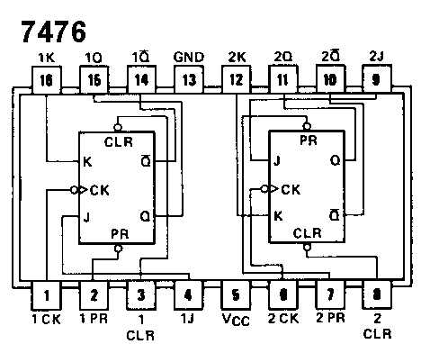
This circuit shows the actual JK flipflop structure used in the TTL-series 7476 bipolar integrated circuit.
Besides the CLOCK, J, and K inputs and the Q and NQ outputs, two extra inputs nPRESET (or set) and nCLEAR (reset) are provided. One 7476 integrated circuit contains two of these flipflops.
When J=K=1,it works in toggle mode.
General description :PNP transistor in a TO-92; SOT54 plastic package.
Features
Low current (max. 100 mA)
Low voltage (max. 65 V).
Applications: General purpose switching and amplification.
A relay is an electrically operated switch. Many relays use an electromagnet to operate a switching mechanism mechanically, but other operating principles are also used. Relays are used where it is necessary to control a circuit by a low-power signal (with complete electrical isolation between control and controlled circuits), or where several circuits must be controlled by one signal. The first relays were used in long distance telegraph circuits, repeating the signal coming in from one circuit and re-transmitting it to another. Relays were used extensively in telephone exchanges and early computers to perform logical operations.
WORKING PRINCIPLE:
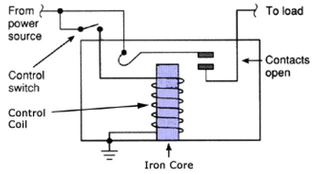
Relay showing coil and switch contacts |
A relay is an electrically operated switch. Current flowing through the coil of the relay creates a magnetic field which attracts a lever and changes the switch contacts. The coil current can be on or off so relays have two switch positions and most have double throw (changeover) switch contacts as shown in the diagram.
Relays allow one circuit to switch a second circuit which can be completely separate from the first. For example a low voltage battery circuit can use a relay to switch a 230V AC mains circuit. There is no electrical connection inside the relay between the two circuits, the link is magnetic and mechanical.
The coil of a relay passes a relatively large current, typically 30mA for a 12V relay, but it can be as much as 100mA for relays designed to operate from lower voltages. Most ICs (chips) cannot provide this current and a transistor is usually used to amplify the small IC current to the larger value required for the relay coil. The maximum output current for the popular 555 timer IC is 200mA so these devices can supply relay coils directly without amplification.
Relays are usuallly SPDT or DPDT but they can have many more sets of switch contacts, for example relays with 4 sets of changeover contacts are readily available. For further information about switch contacts and the terms used to describe them please see the page on switches.
Most relays are designed for PCB mounting but you can solder wires directly to the pins providing you take care to avoid melting the plastic case of the relay.
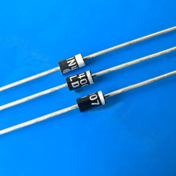
The supplier's catalogue should show you the relay's connections. The coil will be obvious and it may be connected either way round. Relay coils produce brief high voltage 'spikes' when they are switched off and this can destroy transistors and ICs in the circuit. To prevent damage you must connect a protection diode across the relay coil.
The animated picture shows a working relay with its coil and switch contacts. You can see a lever on the left being attracted by magnetism when the coil is switched on. This lever moves the switch contacts. There is one set of contacts (SPDT) in the foreground and another behind them, making the relay DPDT.
The relay's switch connections are usually labelled COM, NC and NO:
· COM = Common, always connect to this, it is the moving part of the switch.
· NC = Normally Closed, COM is connected to this when the relay coil is off.
· NO = Normally Open, COM is connected to this when the relay coil is on.
· Connect to COM and NO if you want the switched circuit to be on when the relay coil is on.
· Connect to COM and NC if you want the switched circuit to be on when the relay coil is off.
Choosing a relay
You need to consider several features when choosing a relay:
- Physical size and pin arrangement
If you are choosing a relay for an existing PCB you will need to ensure that its dimensions and pin arrangement are suitable. You should find this information in the supplier's catalogue. - Coil voltage
The relay's coil voltage rating and resistance must suit the circuit powering the relay coil. Many relays have a coil rated for a 12V supply but 5V and 24V relays are also readily available. Some relays operate perfectly well with a supply voltage which is a little lower than their rated value. - Coil resistance
The circuit must be able to supply the current required by the relay coil. You can use Ohm's law to calculate the current:
Relay coil current = | supply voltage |
coil resistance |
- For example: A 12V supply relay with a coil resistance of 400 passes a current of 30mA. This is OK for a 555 timer IC (maximum output current 200mA), but it is too much for most ICs and they will require a transistor to amplify the current.
- Switch ratings (voltage and current)
The relay's switch contacts must be suitable for the circuit they are to control. You will need to check the voltage and current ratings. Note that the voltage rating is usually higher for AC, for example: "5A at 24V DC or 125V AC". - Switch contact arrangement (SPDT, DPDT etc)
Most relays are SPDT or DPDT which are often described as "single pole changeover" (SPCO) or "double pole changeover" (DPCO). For further information please see the page on switches.
NPN General Purpose Amplifier
CHARACTERISTICS
Thermal Characteristics TA = 25°C unless otherwise noted
Symbol Parameter Value Units
VCEO Collector-Emitter Voltage 30 V
VCES Collector-Base Voltage 30 V
VEBO Emitter-Base Voltage 5.0 V
IC Collector Current - Continuous 500 mA
TJ, Tstg Operating and Storage Junction Temperature Range -55 to +150 C
In the case of semiconductor diodes, the temperature range over which the temperature dependence of the forward voltage is linear, can be increased by lowering the operating current along with the increase of the sensitivity (dVf/dT) which is found to vary logarithmically with I. The temperature and current dependence of forward voltage Vf can be explained by using the theory of the p-n junction. The capacitance-voltage (C−V) measurements of p-n junctions are carried out at different temperatures and are discussed in light of the theory of the p-n junction. The band gap Eg, estimated from Vf−T measurement, is found to be ∼ 1.17 eV, whereas it is found to be 1.189 eV from C−V measurement.
TSOP-1738:
TSOP-1738:
CIRCUIT OF RECEIVER SECTION:
Working of the receiver section:
1. The receiver section uses an infrared sensor module which is commonly used in color television for sensing the IR signals from the transmitter section.
2. The switch S1 of the transmitter is pressed the IR LEDs radiate IR beams with a modulating frequency of 38 KHz .
3. The IR signal from the transmitter is sensed by the sensor and its output at pin 2 goes low switching on the transistor T1and charging the capacitor C5 through R5.
4. When voltage across capacitor C8 reaches about 3.5V, IC 4017 receives a clock pulse at pin 14 and its output at pin2 goes high. This results in forward biasing of transistor T2, which on conduction energises relay RL1 connected at its collector .The output of IC 4017 is also used for lighting LED1, indicating presence of signal.
5. When no signal is available , output of the sensor module goes high and transistor T1 is switched off. Now capacitor C8 starts discharging through resistor R6 and voltage across it gradually decreases to zero.
6. When another signal arrives after about 300ms, capacitor C8 charges again through resistor R5 and pin 14 of IC 4017 is gets another clock pulse .But as Q2 output of IC 4017 is connected to the reset pin 15 through diode D4, the output at pin 2 toggles .That is, IC2 works as a bistable Flipflop.
Modifications and advantages:
The main advantage of this circuit lies in the fact that it can be easily converted into a multichannel remote control system by simply changing the output pin number that is connected to the reset pin of IC 4017, and taking more outputs from the corresponding pins of IC 4017.
I am extremely grateful to our HOD sir (Prof. Supriyo Sengupto)and our mentor for their constant help and valuable guidance.
Bibliography:
1. EFY magazine.
2. www.wikipedia.org
3. www.alldatasheet.com
Subscribe to:
Comments (Atom)


